Devices
Joseph F. Alward, PhD
Department of Physics
University of the Pacific
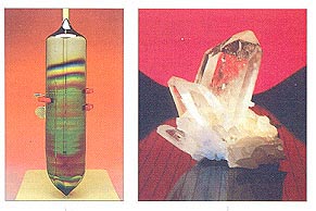
Silicon Crystal Silicon Dioxide
| Semiconductor
Devices Joseph F. Alward, PhD Department of Physics University of the Pacific |
Silicon Crystal Silicon Dioxide |
Important Words and Concepts: Part 1
| charge layers: at the junction
interface, layers of exposed (uncovered, or uncompensated) dopant ions doping: growing crystals with impurities dopant: the impurity element diode: a pn junction hole: an unoccupied bond site of silicon pnp transistor: sandwich of p material with n-type in the middle turn on voltage: the voltage at which the pn junction begins to rise rapidly doping concentration: typically one in a million Si atoms are replaced by As or B |
Diode Rectification: PN junction
diodes permit current to flow in one direction only. Thermal Generation of Electron-Hole Pairs: Thermal energy is often sufficient to dislodge an electron from its silicon parent, leaving behind a hole. Transistors: Small changes in the forward bias near the turn-on voltage of a pn junction leads to large changes in the current. This action is responsible in part for the amplification abilities of a pnp transistor. |
Important Words and Concepts 2I
| junction electric field: Electric field
which exists at the interface of a p- and n-type silicon, caused by the loss of the covering free charge carriers (holes or electrons) which normally orbit nearby. hole movement: a single hole moves throughout the crystal by virtue of hoppings from one Si site to another by many different electrons. photovoltaic devices: devices in which light generates current or voltage. |
The Silicon Crystal
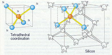 |
Silicon Doped with Arsenic
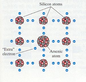 |
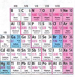 Arsenic is in Group V, which means its outer shell contains five electrons. |
Silicon Doped with Boron
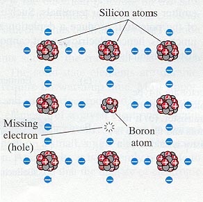 |
Boron is in Group III, which means that its outer shell contains three electrons. |
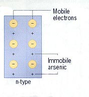
N-Type Silicon
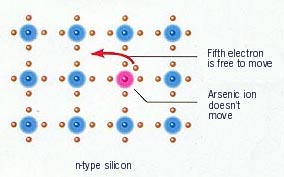 Negative-type charge carriers are added to the silicon crystal, making it "n-type". The crystal is still neutral, however. |
P-Type Silicon
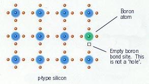 The empty boron bond site will sets up a chain-reaction in which electrons on silicon atoms fill the empty bond site of a neighbor. |
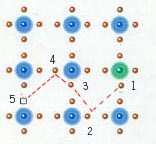
Hole Movement
 Boron is neutral, but nearby electron may jump to fill bond site. |
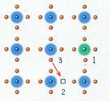 Boron is now a negative ion. |
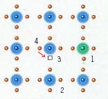 It takes very little thermal energy to kick electrons from one silicon to another silicon. |
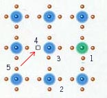 Hole has moved from 2 to 3 to 4, and will soon move to 5. |
Holes are Positive Charge Carriers
 |
The empty silicon bond sites (holes) are thought of as being positive, since their presence makes that region positive. This type of silicon is "p-type". |
N- and P-Type Silicon Diagrams
 The dominant charge carrier in n-type Si is the electron. This crystal is neutral. |
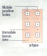 The dominant charge carrier in p-type Si is the hole This crystal is neutral. |
Important Facts:
Not shown are the silicon atoms, |
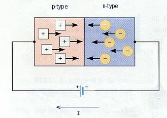
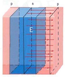
P- and N-Type Silicon Joined
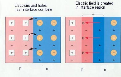 Diffusing holes and electrons create layers of opposite charge in the interface region. |
Charges in the Interface Region
 |
Most of the boron (B-) ions on the p
side are "covered", meaning that swimming about them, on the average, is one hole. Most of the arsenic (As+) ions on the n side are covered by an electron. Near the interface, these ions are uncovered. |
A Forward-Biased PN Junction
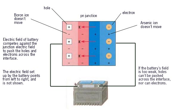 |
Forward-Biased PN Junction
 |
Electric field of battery (not shown)
overwhelms interface electric field (not shown), allowing holes and electrons to be pushed across interface. Such a connection is called a "forward bias", because it allows current to go forward. |
PN Junction Under Reverse Bias
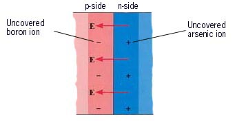
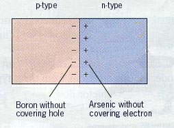 Charge layers were created because holes from the left, and electrons from the right, diffused across the interface, thereby uncovering the dopant ions. |
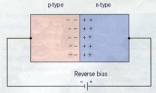
Battery removes more covering holes from the p-side and covering electrons from the n-side, widening the charge layers. |
Negligible Current in Reverse Bias
|
Widening of the charge layers is a consequence of reverse bias, but it's not the cause of the negligibly small current. Reverse- bias layer-widening is important in the field of photovoltaics (discussed later). Reverse current is limited by thermal generation of electron- hole pairs. |
Thermally Generated Reverse Current
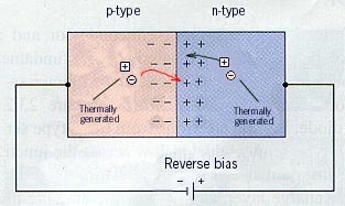 |
Thermal energy (heat) shakes some electrons out of their silicon bond sites, creating a free electrons and a free holes. If thermal generation occurs near the interface, some of the carriers will be swept up by the electric field set up by the charge layers. |
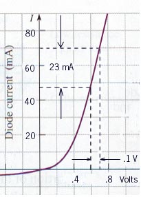
Characteristic Curve
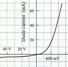 Reverse current exaggerated; typical reverse current: 10 microamperes. |
This is the "characteristic" curve of a pn junction diode. It shows the slow, then abrupt, rise of current as the voltage is raised. Under reverse bias, even very large voltages will cause only very small currents, essentially constant reverse bias currents. The reverse bias current depends mainly on the rate of thermal generation of electron-hole pairs. |
Turn-On Voltage
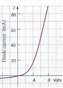 |
A pn junction diode "turns on" at about 0.6 V, but that varies according to the doping concentration. Notice the sharp rise in current near the turn-on voltage. This behavior will be exploited later in the construction of the transistor amplifier. |
A PN Junction Diode and Its Symbol
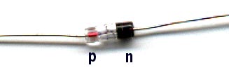 Black band corresponds to the "point" in the diode symbol on the right. |
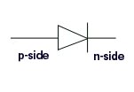 It points as "point" is spelled, with "p" first, and"n" later. |
Rectification of an AC Signal
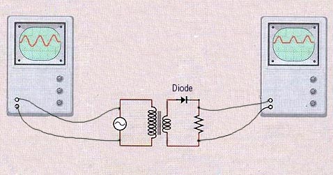 |
Rectification Explained
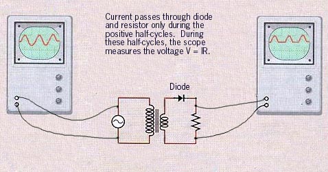 |
Smoothing the Rectified Signal
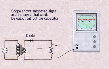 |
Capacitor charges up during the positive half-cycle, then releases its charge through the resistor during the negative half-cycle, causing current through the resistor that otherwise wouldn't exist. 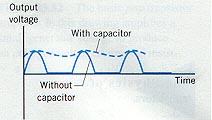 |
Bipolar Junction Transistors
Bipolar junction transistors (BJT). Two types of charge carriers are involved. |
| The junction on the left side of the base is forward-biased; the junction on the right side of the base is reverse-biased. Base is very narrow, and not drawn to scale. |
| Large electric field exists at the collector junction interface. |
 Holes entering narrow base are swept into collector by the electric field. |
Amplification with the Bipolar Junction Transistor
| Emitter-base junction is biased at the turn-on voltage, so even very small changes in voltage there will lead to very large changes in the emitter-base current (see detail). Electric field at the base-collector junction sweeps up almost all holes which enter the base. Weak input signal is amplified by |
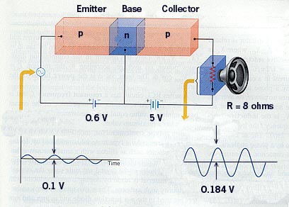 Voltage across speaker resistor is IR. DV = R DI |
DV = R D I |
Photovoltaic Devices
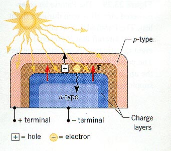 |
Light energy absorbed by an electron in a silicon bond site will kick the electron out of the bond, creating a free electron and a free hole. If this electron-hole pair is created in the charge-layer region, the electric field will sweep the oppositely-charged carriers in opposite directions. Voltages which are generated by light are called photovoltaic devices. |
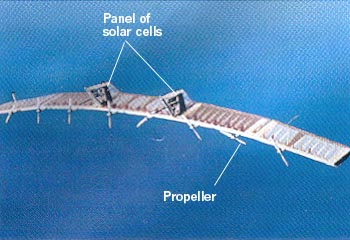
Pathfinder Solar Powered Aircraft
 |
Appendix
|
A pn junction diode "turns on" at about 0.6 V, but that varies according to doping concentration. Notice the sharp rise in current near the turn-on voltage. This behavior will be exploited later in the construction of the transistor amplifier. |